Spectroscopic techniques have pushed the materials research a notch ahed, whether its grain boundary segregation or higher phosphorus content in steel, spectroscopy have proved to be determining tool in these field of research. Secondary ion mass spectroscopy is another such technique used primarily for determining diffusion of elements inside a material through various processes. Whether its lattice or grain boundary diffusion, whether it’s a two phase material or a single phase, SIMS has provided very accurate diffusivity measurement.
How it works? Well the mechanism sounds quite simple but the instrumentation is not so simple. An ion beam is used for scan over the surface of the specimen. This powerful beam of O+, Cs+, or O- takes out material from the surface of specimen. O2 or Cs gases are ionized in duplasmtron and using few electrostatic lenses they are focused on the specimen. This beam ionizes the materials from the surface and takes out materials from the specimens. After the ions flies from the surface, they travel under a potential different. Lenses and filters take out the high energy ions from the ion flow. These ions are mass separated in a magnetic separator where the ions are separated depending on their mass to charge ratio. Another technique used for mass separating the ions is through quadrapole where crtical voltages are applied to separate specific ions. In case of magnetic separator the trajectories of the flying ions are exploited, the ions with different mass to charge ratio have different trajectories.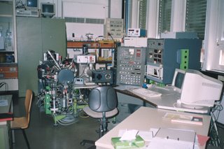


Schematic of the column in which the ion moves. courtesy Cameca
The crater which forms due to the rastering of the ion beam covers a region of 250 250 µm. The depth resolution of this instrument sometimes will be as high as 1-2 nm. New generation SIMS now-a-days provides secondary electron imaging facility, so it is possible to identify phases or elemental changes in the material. This technique is also useful for studying interfaces in the semiconductor devices or measure lattice and grain boundary diffusivity independently. A major use of SIMS is in locating impurities in the materials, xray spectroscopy or other spectroscopic technique many a time fail to present the information that can be achievable through SIMS.
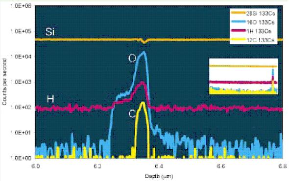 Presence of C and O impurities in a bonded Si wafer. Courtsey Ansto
Many companies in the world make SIMS, as I took picture from the web pages of companies I am providing the link below.
Cameca
Ansto
No comments:
Post a Comment